SNVAAA8 September 2025 LM3478 , LM3478Q-Q1 , LM3481 , LM3481-Q1 , LM5155 , LM5155-Q1 , LM5156 , LM5156-Q1 , LM5157 , LM5157-Q1 , LM5158 , LM5158-Q1 , TPS40210 , TPS40210-Q1
Introduction
While a synchronous boost converter can allow negative currents through the high-side switch in fixed pulse width modulation (FPWM) operation, an asynchronous converter uses a diode which blocks current flow in reverse direction. In addition, each converter has a minimum on-time of the driver, meaning there is a minimum amount of power that is transferred to the output with each switching cycle. During light load conditions, it is possible that the required output power is smaller than the amount delivered each cycle, so the excessive power leads to an increase in output voltage instead. To avoid an increase of output voltage, the converter stops switching in this situation and enters a pulse-skip mode.
While pulse-skip mode has the advantage of increased efficiency, the negative effect is that the device no longer switches with fixed frequency. An increase of the output voltage ripple and worse EMI performance can contradict the design goals, so pulse-skip mode is not necessarily desired for every application.
An asynchronous converter keeps operation with fixed frequency for as long as the required duty cycle (and therefore the driver on-time) does not drop below the supported minimum on-time of the device. The minimum on-time is specified in the electrical characteristics of the data sheet. If a smaller duty cycle is required to keep a constant output voltage, the device reduces the duty cycle until the minimum on-time is reached and then enters skip-mode as soon as the output voltage increases above target. The exact conditions for skip-mode can vary between devices.
For example, the LM3478 keeps operation with minimum on-time while the output voltage is increasing up to the overvoltage protection (OVP) threshold and then enters a stand-by state where the device stops switching until VOUT drops below a hysteresis threshold. Newer devices such as LM5158 achieve smaller VOUT ripple by not only monitoring the feedback voltage for OVP, but also the COMP pin and current sense pin voltage level to enter skip-mode operation when the COMP level drops below a certain threshold.
Implementation
Equation 1 calculates the required duty cycle and Equation 2 computes the driver on-time.
where
- DDCM is the duty cycle in discontinuous conduction mode
- ton is the on-time of the gate driver
Input voltage (VIN) and output voltage (VOUT) are given by the application requirements and the minimum on-time is given by the device specification. The output load (IOUT) can be increased by adding a dummy load, but this reduces overall efficiency. Inductance (L) and switching frequency (FSW) are the parameters that can be adjusted more freely.
A slower switching frequency increases both on-time and off-time of the driver while not affecting the duty cycle. As the minimum on-time of the controller is an absolute value (nanoseconds), pulse skipping can be avoided with this approach.
However, note that the LM515x series has a minimum on-time parameter that changes over switching frequency. This reduces the impact of a FSW change.
Increasing the inductance directly increases the duty cycle and therefore the on-time of the driver. The disadvantage of higher inductance is an increase in component size, stronger bandwidth limitation of the loop response, and lower current ripple at high loads. The latter comes with the risk of instability at high-load operation, as peak-current-mode control needs some degree of current ripple to read a proper current-sense slope.
Test Results
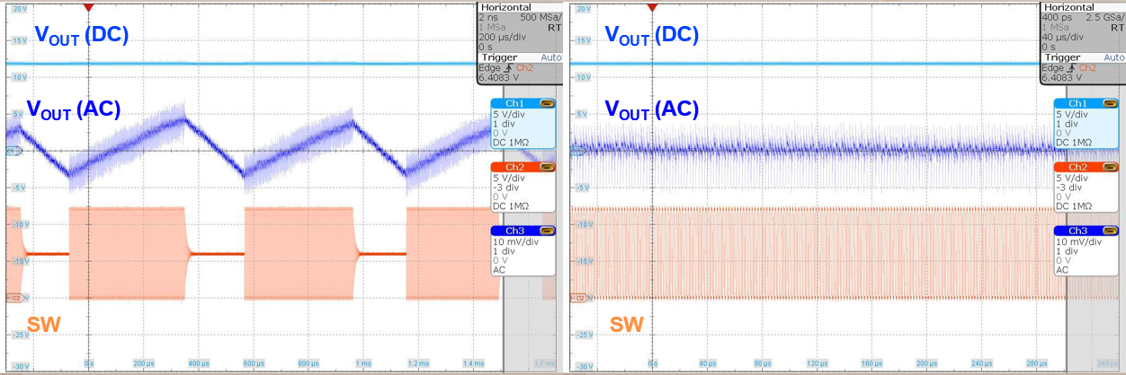
The LM5158 boost converter device states a minimum on-time of 80ns (typical) at 2.2MHz switching frequency. For this device, the minimum on-time increases with lower switching frequency. To be precise, the decrease of the required minimum on-time with higher switching frequency aligns directly with minimum on-time capabilities of the converter, so no difference is observed on the pulse-skip behavior with a change in FSW.


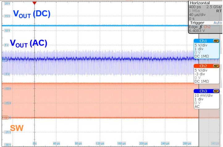
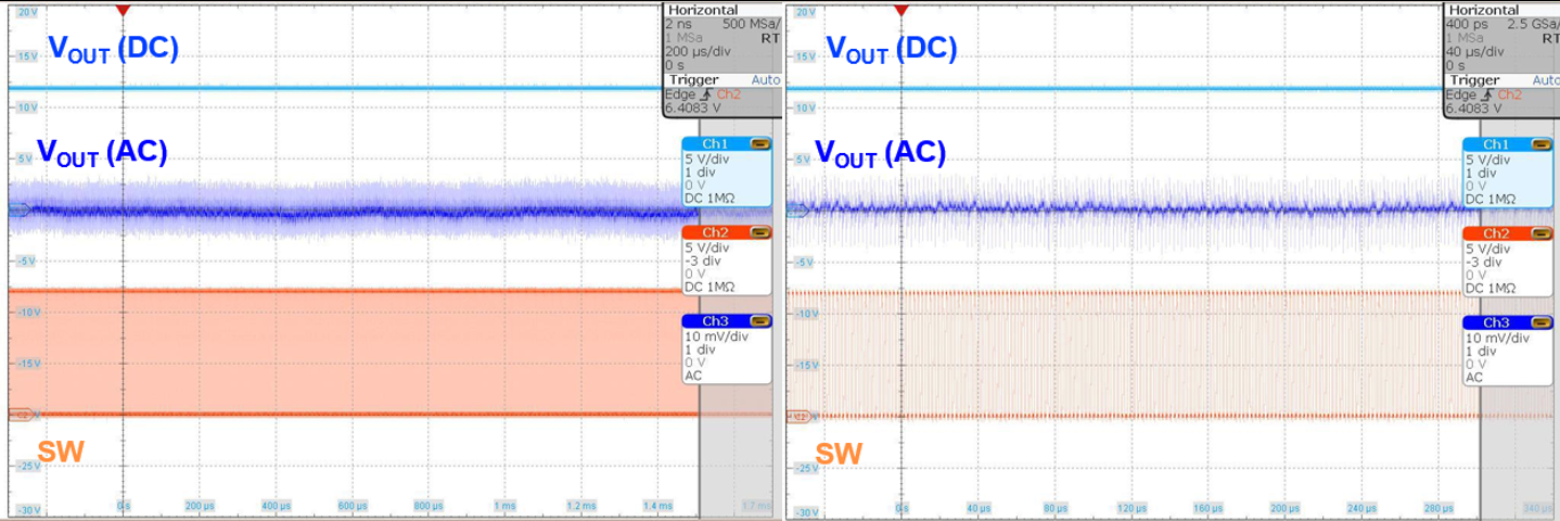
However, increasing the inductance in the LM5158 design shows the expected change of shifting the skip mode threshold to lower loads. In this case, the design now continues PWM operation even at zero load condition.

The minimum on-time of LM3481 is not variable over switching frequency. Because of this, a different skip mode threshold is observed after increasing the switching frequency.
Increasing the inductance shows the same result of skip mode threshold shift.


Conclusion
The pulse-skip operation is necessary in an asynchronous boost design to avoid an increase of VOUT during light load conditions. Even in a synchronous boost design, skip-mode operation is useful to increase light load efficiency. This phenomenon is also seen in other topologies like SEPIC or Flyback converters.
Understanding the equation to calculate the expected on-time and possible parameters to increase this value above the minimum on-time limitation of the device shows potential design adjustments to avoid pulse-skip operation for all operation conditions.
References
Texas Instruments, Under the Hood of a DC/DC Boost Converter, Brian T. Lynch