SLLS519J March 2002 – July 2017 TUSB3410
PRODUCTION DATA.
- 1Device Overview
- 2Revision History
- 3Pin Configuration and Functions
- 4Specifications
-
5Detailed Description
- 5.1 Overview
- 5.2 Functional Block Diagram
- 5.3 Device Functional Modes
- 5.4 Processor Subsystems
- 5.5
Memory
- 5.5.1 MCU Memory Map
- 5.5.2 Registers
- 5.5.3 Buffers + I/O RAM Map
- 5.5.4
Endpoint Descriptor Block (EDB−1 to EDB−3)
- 5.5.4.1 OEPCNF_n: Output Endpoint Configuration (n = 1 to 3) (Base Addr: FF08h, FF10h, FF18h)
- 5.5.4.2 OEPBBAX_n: Output Endpoint X-Buffer Base Address (n = 1 to 3) (Offset 1)
- 5.5.4.3 OEPBCTX_n: Output Endpoint X Byte Count (n = 1 to 3) (Offset 2)
- 5.5.4.4 OEPBBAY_n: Output Endpoint Y-Buffer Base Address (n = 1 to 3) (Offset 5)
- 5.5.4.5 OEPBCTY_n: Output Endpoint Y-Byte Count (n = 1 to 3) (Offset 6)
- 5.5.4.6 OEPSIZXY_n: Output Endpoint X-/Y-Buffer Size (n = 1 to 3) (Offset 7)
- 5.5.4.7 IEPCNF_n: Input Endpoint Configuration (n = 1 to 3) (Base Addr: FF48h, FF50h, FF58h)
- 5.5.4.8 IEPBBAX_n: Input Endpoint X-Buffer Base Address (n = 1 to 3) (Offset 1)
- 5.5.4.9 IEPBCTX_n: Input Endpoint X-Byte Count (n = 1 to 3) (Offset 2)
- 5.5.4.10 IEPBBAY_n: Input Endpoint Y-Buffer Base Address (n = 1 to 3) (Offset 5)
- 5.5.4.11 IEPBCTY_n: Input Endpoint Y-Byte Count (n = 1 to 3) (Offset 6)
- 5.5.4.12 IEPSIZXY_n: Input Endpoint X-/Y-Buffer Size (n = 1 to 3) (Offset 7)
- 5.5.4.13 Endpoint-0 Descriptor Registers
- 5.5.5
USB Registers
- 5.5.5.1 FUNADR: Function Address Register (Addr:FFFFh)
- 5.5.5.2 USBSTA: USB Status Register (Addr:FFFEh)
- 5.5.5.3 USBMSK: USB Interrupt Mask Register (Addr:FFFDh)
- 5.5.5.4 USBCTL: USB Control Register (Addr:FFFCh)
- 5.5.5.5 MODECNFG: Mode Configuration Register (Addr:FFFBh)
- 5.5.5.6 Clock Output Control
- 5.5.5.7 Vendor ID/Product ID
- 5.5.5.8 SERNUM7: Device Serial Number Register (Byte 7) (Addr:FFEFh)
- 5.5.5.9 SERNUM6: Device Serial Number Register (Byte 6) (Addr:FFEEh)
- 5.5.5.10 SERNUM5: Device Serial Number Register (Byte 5) (Addr:FFEDh)
- 5.5.5.11 SERNUM4: Device Serial Number Register (Byte 4) (Addr:FFECh)
- 5.5.5.12 SERNUM3: Device Serial Number Register (Byte 3) (Addr:FFEBh)
- 5.5.5.13 SERNUM2: Device Serial Number Register (Byte 2) (Addr:FFEAh)
- 5.5.5.14 SERNUM1: Device Serial Number Register (Byte 1) (Addr:FFE9h)
- 5.5.5.15 SERNUM0: Device Serial Number Register (Byte 0) (Addr:FFE8h)
- 5.5.5.16 Function Reset and Power-Up Reset Interconnect
- 5.5.5.17 Pullup Resistor Connect and Disconnect
- 5.5.6
DMA Controller Registers
- 5.5.6.1 DMACDR1: DMA Channel Definition Register (UART Transmit Channel) (Addr:FFE0h)
- 5.5.6.2 DMACSR1: DMA Control And Status Register (UART Transmit Channel) (Addr:FFE1h)
- 5.5.6.3 DMACDR3: DMA Channel Definition Register (UART Receive Channel) (Addr:FFE4h)
- 5.5.6.4 DMACSR3: DMA Control And Status Register (UART Receive Channel) (Addr:FFE5h)
- 5.5.7
UART Registers
- 5.5.7.1 RDR: Receiver Data Register (Addr:FFA0h)
- 5.5.7.2 TDR: Transmitter Data Register (Addr:FFA1h)
- 5.5.7.3 LCR: Line Control Register (Addr:FFA2h)
- 5.5.7.4 FCRL: UART Flow Control Register (Addr:FFA3h)
- 5.5.7.5 Transmitter Flow Control
- 5.5.7.6 MCR: Modem-Control Register (Addr:FFA4h)
- 5.5.7.7 LSR: Line-Status Register (Addr:FFA5h)
- 5.5.7.8 MSR: Modem-Status Register (Addr:FFA6h)
- 5.5.7.9 DLL: Divisor Register Low Byte (Addr:FFA7h)
- 5.5.7.10 DLH: Divisor Register High Byte (Addr:FFA8h)
- 5.5.7.11 Baud-Rate Calculation
- 5.5.7.12 XON: Xon Register (Addr:FFA9h)
- 5.5.7.13 XOFF: Xoff Register (Addr:FFAAh)
- 5.5.7.14 MASK: UART Interrupt-Mask Register (Addr:FFABh)
- 5.5.8 Expanded GPIO Port
- 5.5.9 Interrupts
- 5.5.10 I2C Registers
- 5.6
Boot Modes
- 5.6.1 Introduction
- 5.6.2 Bootcode Programming Flow
- 5.6.3 Default Bootcode Settings
- 5.6.4 External I2C Device Header Format
- 5.6.5 Checksum in Descriptor Block
- 5.6.6 Header Examples
- 5.6.7 USB Host Driver Downloading Header Format
- 5.6.8 Built-In Vendor Specific USB Requests
- 5.6.9 Bootcode Programming Consideration
- 5.6.10 File Listings
- 6Application, Implementation, and Layout
- 7Device and Documentation Support
- 8Mechanical Packaging and Orderable Information
封裝選項(xiàng)
機(jī)械數(shù)據(jù) (封裝 | 引腳)
散熱焊盤機(jī)械數(shù)據(jù) (封裝 | 引腳)
- RHB|32
訂購信息
6 Application, Implementation, and Layout
NOTE
Information in the following applications sections is not part of the TI component specification, and TI does not warrant its accuracy or completeness. TI’s customers are responsible for determining suitability of components for their purposes. Customers should validate and test their design implementation to confirm system functionality.
6.1 Application Information
The implementation in Section 6.2 describes the minimum requirements to set up the TUSB3410 device for use as a basic USB to UART bridge to link the communication of a PC to any serial device through a USB port (see Figure 6-1).
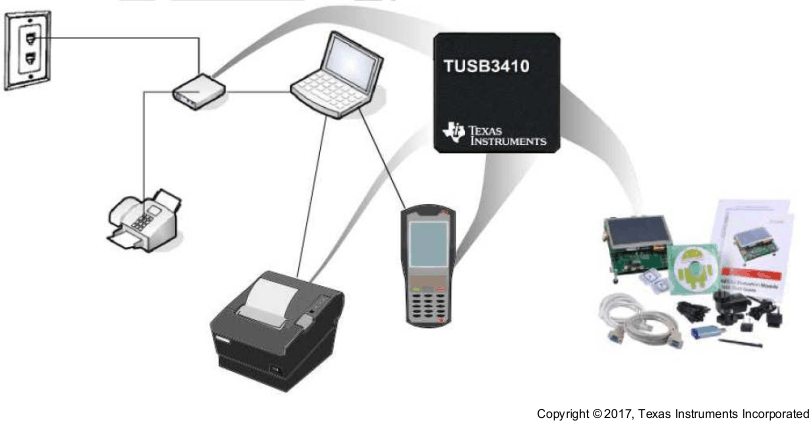 Figure 6-1 Typical Example for TUSB3410 as USB to UART Bridge
6.2 Typical Application
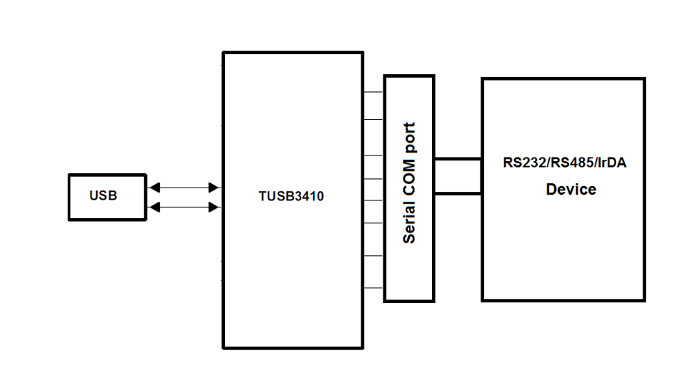 Figure 6-2 USB to UART Implementation
6.2.1 Design Requirements
Table 6-1 lists the design parameters for the typical application shown in Section 6.2.
Table 6-1 Design Parameters
| DESIGN PARAMETER | VALUE |
|---|---|
| VCC Supply | 3.3 V |
| VDD1/8 | 1.8 V |
| Upstream port USB (HS, FS) | HS, FS |
| RS-232 Transceivers | RS-232 |
| XTAL | 12 MHz |
6.2.2 Detailed Design Procedure
6.2.2.1 Upstream Port Implementation
Figure 6-3 shows how the upstream of the TUSB3410 device is connected to a USB-2.0 Type B connector. The VBUS of the USB-2.0 connector is connected to a 3.3-V voltage regulator, which generates the 3.3 V required for VCC. The 3.3 V generated by this voltage regulator will pass through a voltage divider to generate the 1.8 V that is required for VDD.
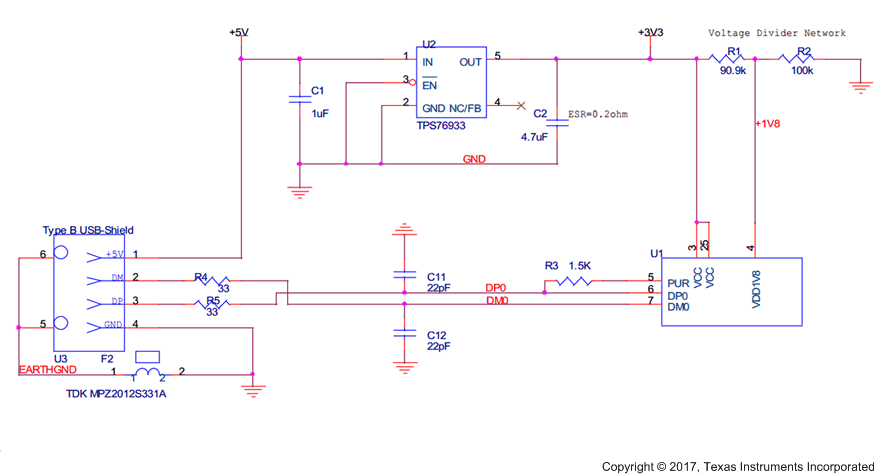 Figure 6-3 Upstream Port Implementation Schematic
6.2.2.2 Crystal Implementation
The TUSB3410 device requires a 12-MHz clock source to work properly, which is placed across the X1 and X2 terminals as shown in Figure 6-4.
TI recommends using a parallel-resonant crystal. Most parallel-resonant crystals are specified at a frequency with a load capacitance of 18 pF. This load can be realized by placing 33-pF capacitors from each end of the crystal to ground. Together with the input capacitance of the TUSB3410 device and stray board capacitance, this setup provides close to two 36-pF capacitors in series to emulate the 18-pF load requirement.
 Figure 6-4 Crystal Implementation Schematic
6.2.2.3 RS-232 Implementation
All the serial data lines and serial control signals (DTR, RTS, SOUT/IR_SOUT, SIN/IR_SIN, RI/CP, DCD, DSR, and CTS) must go through an RS-232 driver (see Figure 6-5). For this example, the SN75LV4737A device is used (see SLLS178 for more details about the RS-232 driver). After the RS-232 driver is placed, the serial data lines and serial control signals are connected to a DB9 connector.
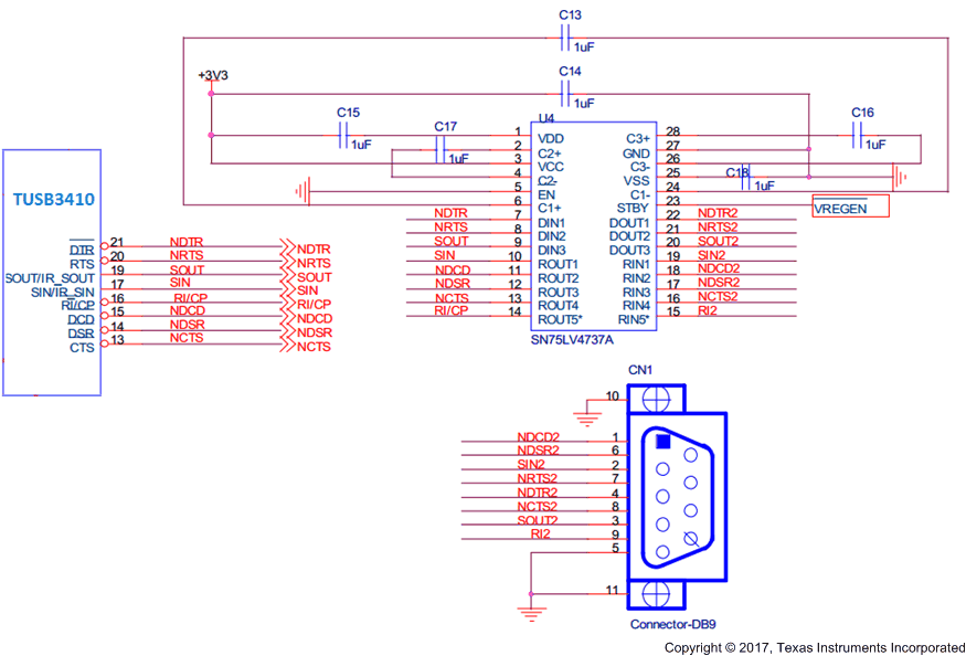 Figure 6-5 RS-232 Implementation Schematic
6.2.2.4 TUSB3410 Power Implementation
Figure 6-6 shows the power implementation for the TUSB3410 device.
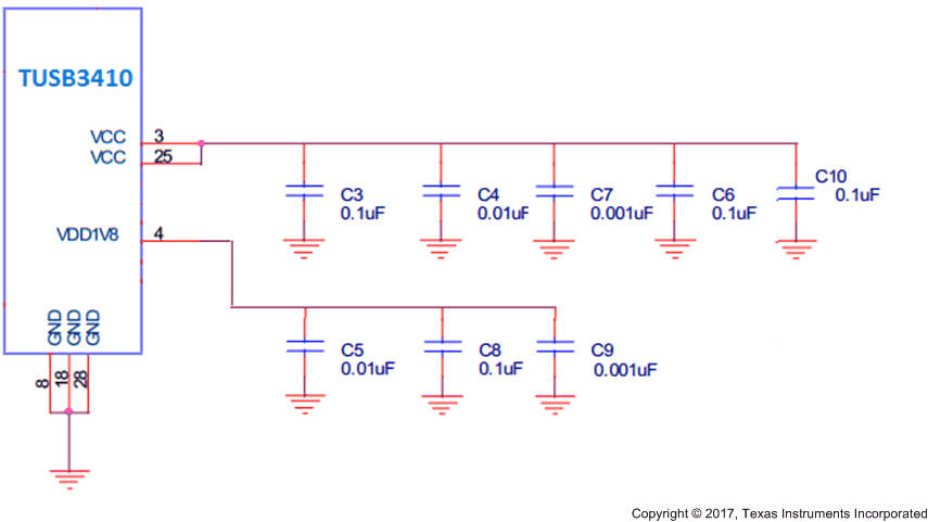 Figure 6-6 Power Implementation
6.2.3 Application Performance Plot
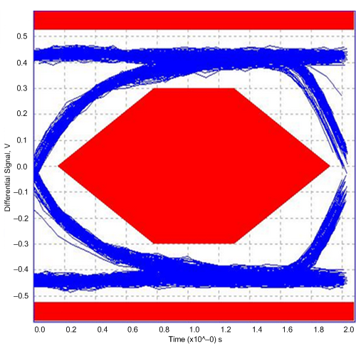 Figure 6-7 High-Speed Upstream Port
6.3 Layout
6.3.1 Layout Guidelines
A primary concern when designing a system is accommodating and isolating high-speed signals. As highspeed signals are most likely to impact or be impacted by other signals, they must be laid out early (preferably first) in the PCB design process to ensure that prescribed routing rules can be followed. Table 6-2 outlines the signals requiring the most attention in a USB layout.
Table 6-2 Critical Signals
| SIGNAL NAME | DESCRIPTION |
|---|---|
| DP | USB 2.0 differential pair, positive |
| DM | USB 2.0 differential pair, negative |
| SSTXP | SuperSpeed differential pair, TX, positive |
| SSTXN | SuperSpeed differential pair, TX, negative |
| SSRXP | SuperSpeed differential pair, RX, positive |
| SSRXN | SuperSpeed differential pair, RX, negative |
Use the following routing and placement guidelines when laying out a new design for the USB physical layer (PHY). These guidelines help minimize signal quality and electromagnetic interference (EMI) problems on a four-or-more layer evaluation module (EVM).
- Place the USB PHY and major components on the un-routed board first.
- Route the high-speed clock and high-speed USB differential signals with minimum trace lengths.
- Route the high-speed USB signals on the plane closest to the ground plane, whenever possible.
- Route the high-speed USB signals using a minimum of vias and corners. This reduces signal reflections and impedance changes.
- When it becomes necessary to turn 90°, use two 45° turns or an arc instead of making a single 90° turn. This reduces reflections on the signal traces by minimizing impedance discontinuities.
- Do not route USB traces under or near crystals, oscillators, clock signal generators, switching regulators, mounting holes, magnetic devices or ICs that use or duplicate clock signals.
- Avoid stubs on the high-speed USB signals because they cause signal reflections. If a stub is unavoidable, then the stub should be less than 200 mils.
- Route all high-speed USB signal traces over continuous planes (VCC or GND), with no interruptions. Avoid crossing over anti-etch, commonly found with plane splits.
6.3.2 Differential Signal Spacing
To minimize crosstalk in USB implementations, the spacing between the signal pairs must be a minimum of 5 times the width of the trace. This spacing is the 5W rule. Also, maintain a minimum keep-out area of 30 mils to any other signal throughout the length of the trace. Where the USB differential pair abuts a clock or a periodic signal, increase this keep-out to a minimum of 50 mils to ensure proper isolation. Figure 6-8 shows an example of USB2 differential signal spacing.
 Figure 6-8 USB2 Differential Signal Spacing (mils)
6.3.3 Differential Signal Rules
- Do not place probe or test points on any USB differential signal.
- Do not route USB traces under or near crystals, oscillators, clock signal generators, switching power regulators, mounting holes, magnetic devices, or ICs that use or duplicate clock signals.
- After BGA breakout, keep USB differential signals clear of the SoC because high current transients produced during internal state transitions can be difficult to filter out.
- When possible, route the USB differential pair signals on the top or bottom layer of the PCB with an adjacent GND layer. TI does not recommend stripline routing of the USB differential signals.
- Ensure that USB differential signals are routed ≥ 90 mils from the edge of the reference plane.
- Ensure that USB differential signals are routed at least 1.5 W (calculated trace-width × 1.5) away from voids in the reference plane. This rule does not apply where SMD pads on the USB differential signals are voided.
- Maintain constant trace width after the SoC BGA escape to avoid impedance mismatches in the transmission lines.
- Maximize differential pair-to-pair spacing when possible.
For specific USB-2.0 layout guidelines, refer to USB Layout Guidelines (SPRAAR7).
6.3.4 Layout Example
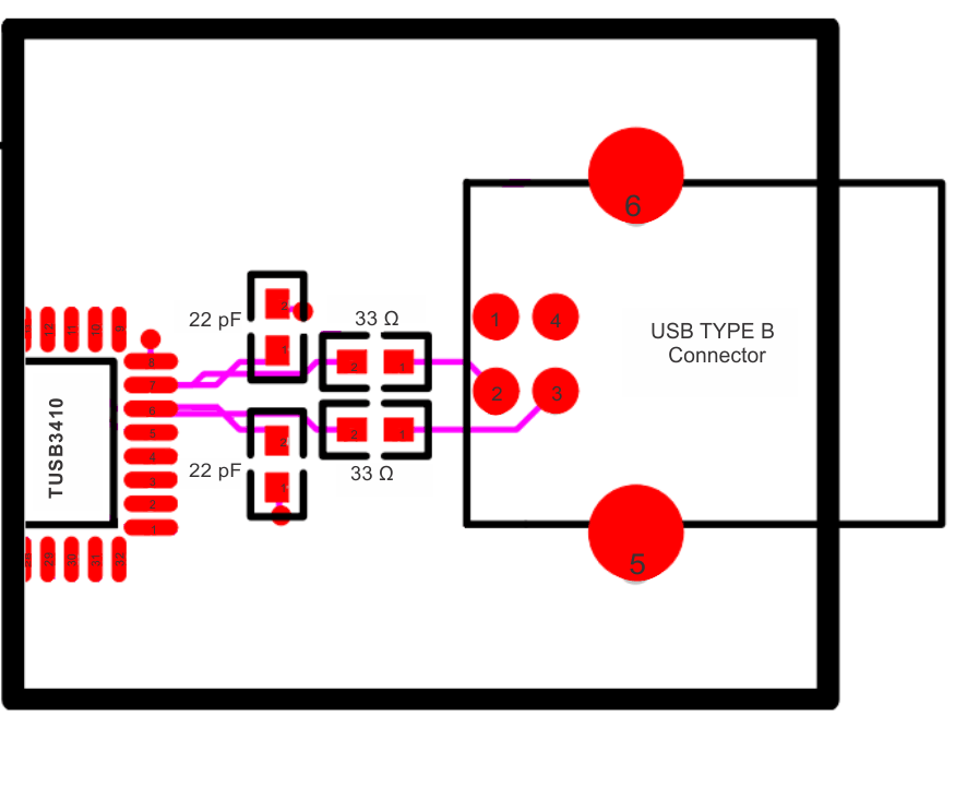 Figure 6-9 Layout Example for TUSB3410
6.4 Power Supply Recommendations
6.4.1 Digital Supplies 3.3 V
The TUSB3410 requires a 3.3-V digital power source.
The 3.3-V terminals are named VCC and supply power to most of the input and output cells. VCC supplies must have 0.1-μF bypass capacitors to VSS (ground) to ensure proper operation. One capacitor per power terminal is sufficient and should be placed as close to the terminal as possible to minimize trace length. TI also recommends smaller value capacitors like 0.01-μF on the digital supply terminals.
When placing and connecting all bypass capacitors, follow high-speed board design rules.
6.4.2 Digital Supplies 1.8 V
The TUSB3410 requires a 1.8-V digital power source.
The 3.3-V terminals are named VDD18 and supply power to most of the input and output cells. VDD18 supplies must have 0.1-μF bypass capacitors to VSS (ground) to ensure proper operation. One capacitor per power terminal is sufficient and should be placed as close to the terminal as possible to minimize trace length. TI also recommends smaller value capacitors like 0.01-μF on the digital supply terminals.
When placing and connecting all bypass capacitors, follow high-speed board design rules.
An internal voltage regulator generates this supply voltage when terminal VREGEN is low. When VREGEN is high, 1.8 V must be supplied externally.
6.5 Crystal Selection
The TUSB3410 device requires a 12-MHz clock source to work properly (see Figure 6-10). This clock source can be a crystal placed across the X1 and X2 terminals. A parallel resonant crystal is recommended. Most parallel resonant crystals are specified at a frequency with a load capacitance of
18 pF. This load can be realized by placing 33-pF capacitors from each end of the crystal to ground. Together with the input capacitance of the TUSB3410 device and stray board capacitance, this provides close to two 36-pF capacitors in series to emulate the 18-pF load requirement.
NOTE
When using a crystal, it takes about 2 ms after power up for a stable clock to be produced.
When using a clock oscillator, the signal applied to the X1/CLKI terminal must not exceed 1.8 V. In this configuration, the X2 terminal is unconnected.
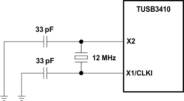 Figure 6-10 Crystal Selection
6.6 External Circuit Required for Reliable Bus Powered Suspend Operation
TI has found a potential problem with the action of the SUSPEND output terminal immediately after power on. In some cases the SUSPEND terminal can power up asserted high. When used in a bus powered application this can cause a problem because the VREGEN input is usually connected to the SUSPEND output. This in turn causes the internal 1.8-V voltage regulator to shut down, which means an external crystal may not have time to begin oscillating, thus the device will not initialize itself correctly.
TI has determined that using components R2 and D1 (rated to 25 mA) in the circuit shown in Figure 6-11 can be used as a workaround.
NOTE
R1 and C1 are required components for proper reset operation, unless the reset signal is provided by another means.
Use of an external oscillator (1.8-V output) versus a crystal would avoid this situation. Self-powered applications would probably not see this problem because the VREGEN input would likely be tied low, enabling the internal 1.8-V regulator at all times.
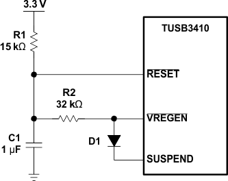 Figure 6-11 External Circuit