SLLS519J March 2002 – July 2017 TUSB3410
PRODUCTION DATA.
- 1Device Overview
- 2Revision History
- 3Pin Configuration and Functions
- 4Specifications
-
5Detailed Description
- 5.1 Overview
- 5.2 Functional Block Diagram
- 5.3 Device Functional Modes
- 5.4 Processor Subsystems
- 5.5
Memory
- 5.5.1 MCU Memory Map
- 5.5.2 Registers
- 5.5.3 Buffers + I/O RAM Map
- 5.5.4
Endpoint Descriptor Block (EDB−1 to EDB−3)
- 5.5.4.1 OEPCNF_n: Output Endpoint Configuration (n = 1 to 3) (Base Addr: FF08h, FF10h, FF18h)
- 5.5.4.2 OEPBBAX_n: Output Endpoint X-Buffer Base Address (n = 1 to 3) (Offset 1)
- 5.5.4.3 OEPBCTX_n: Output Endpoint X Byte Count (n = 1 to 3) (Offset 2)
- 5.5.4.4 OEPBBAY_n: Output Endpoint Y-Buffer Base Address (n = 1 to 3) (Offset 5)
- 5.5.4.5 OEPBCTY_n: Output Endpoint Y-Byte Count (n = 1 to 3) (Offset 6)
- 5.5.4.6 OEPSIZXY_n: Output Endpoint X-/Y-Buffer Size (n = 1 to 3) (Offset 7)
- 5.5.4.7 IEPCNF_n: Input Endpoint Configuration (n = 1 to 3) (Base Addr: FF48h, FF50h, FF58h)
- 5.5.4.8 IEPBBAX_n: Input Endpoint X-Buffer Base Address (n = 1 to 3) (Offset 1)
- 5.5.4.9 IEPBCTX_n: Input Endpoint X-Byte Count (n = 1 to 3) (Offset 2)
- 5.5.4.10 IEPBBAY_n: Input Endpoint Y-Buffer Base Address (n = 1 to 3) (Offset 5)
- 5.5.4.11 IEPBCTY_n: Input Endpoint Y-Byte Count (n = 1 to 3) (Offset 6)
- 5.5.4.12 IEPSIZXY_n: Input Endpoint X-/Y-Buffer Size (n = 1 to 3) (Offset 7)
- 5.5.4.13 Endpoint-0 Descriptor Registers
- 5.5.5
USB Registers
- 5.5.5.1 FUNADR: Function Address Register (Addr:FFFFh)
- 5.5.5.2 USBSTA: USB Status Register (Addr:FFFEh)
- 5.5.5.3 USBMSK: USB Interrupt Mask Register (Addr:FFFDh)
- 5.5.5.4 USBCTL: USB Control Register (Addr:FFFCh)
- 5.5.5.5 MODECNFG: Mode Configuration Register (Addr:FFFBh)
- 5.5.5.6 Clock Output Control
- 5.5.5.7 Vendor ID/Product ID
- 5.5.5.8 SERNUM7: Device Serial Number Register (Byte 7) (Addr:FFEFh)
- 5.5.5.9 SERNUM6: Device Serial Number Register (Byte 6) (Addr:FFEEh)
- 5.5.5.10 SERNUM5: Device Serial Number Register (Byte 5) (Addr:FFEDh)
- 5.5.5.11 SERNUM4: Device Serial Number Register (Byte 4) (Addr:FFECh)
- 5.5.5.12 SERNUM3: Device Serial Number Register (Byte 3) (Addr:FFEBh)
- 5.5.5.13 SERNUM2: Device Serial Number Register (Byte 2) (Addr:FFEAh)
- 5.5.5.14 SERNUM1: Device Serial Number Register (Byte 1) (Addr:FFE9h)
- 5.5.5.15 SERNUM0: Device Serial Number Register (Byte 0) (Addr:FFE8h)
- 5.5.5.16 Function Reset and Power-Up Reset Interconnect
- 5.5.5.17 Pullup Resistor Connect and Disconnect
- 5.5.6
DMA Controller Registers
- 5.5.6.1 DMACDR1: DMA Channel Definition Register (UART Transmit Channel) (Addr:FFE0h)
- 5.5.6.2 DMACSR1: DMA Control And Status Register (UART Transmit Channel) (Addr:FFE1h)
- 5.5.6.3 DMACDR3: DMA Channel Definition Register (UART Receive Channel) (Addr:FFE4h)
- 5.5.6.4 DMACSR3: DMA Control And Status Register (UART Receive Channel) (Addr:FFE5h)
- 5.5.7
UART Registers
- 5.5.7.1 RDR: Receiver Data Register (Addr:FFA0h)
- 5.5.7.2 TDR: Transmitter Data Register (Addr:FFA1h)
- 5.5.7.3 LCR: Line Control Register (Addr:FFA2h)
- 5.5.7.4 FCRL: UART Flow Control Register (Addr:FFA3h)
- 5.5.7.5 Transmitter Flow Control
- 5.5.7.6 MCR: Modem-Control Register (Addr:FFA4h)
- 5.5.7.7 LSR: Line-Status Register (Addr:FFA5h)
- 5.5.7.8 MSR: Modem-Status Register (Addr:FFA6h)
- 5.5.7.9 DLL: Divisor Register Low Byte (Addr:FFA7h)
- 5.5.7.10 DLH: Divisor Register High Byte (Addr:FFA8h)
- 5.5.7.11 Baud-Rate Calculation
- 5.5.7.12 XON: Xon Register (Addr:FFA9h)
- 5.5.7.13 XOFF: Xoff Register (Addr:FFAAh)
- 5.5.7.14 MASK: UART Interrupt-Mask Register (Addr:FFABh)
- 5.5.8 Expanded GPIO Port
- 5.5.9 Interrupts
- 5.5.10 I2C Registers
- 5.6
Boot Modes
- 5.6.1 Introduction
- 5.6.2 Bootcode Programming Flow
- 5.6.3 Default Bootcode Settings
- 5.6.4 External I2C Device Header Format
- 5.6.5 Checksum in Descriptor Block
- 5.6.6 Header Examples
- 5.6.7 USB Host Driver Downloading Header Format
- 5.6.8 Built-In Vendor Specific USB Requests
- 5.6.9 Bootcode Programming Consideration
- 5.6.10 File Listings
- 6Application, Implementation, and Layout
- 7Device and Documentation Support
- 8Mechanical Packaging and Orderable Information
封裝選項
機械數(shù)據(jù) (封裝 | 引腳)
散熱焊盤機械數(shù)據(jù) (封裝 | 引腳)
- RHB|32
訂購信息
4 Specifications
4.1 Absolute Maximum Ratings
over operating free-air temperature range (unless otherwise noted)(1)| MIN | MAX | UNIT | |||
|---|---|---|---|---|---|
| VCC | Supply voltage | −0.5 | 3.6 | V | |
| VI | Input voltage | −0.5 | VCC + 0.5 | V | |
| VO | Output voltage | −0.5 | VCC + 0.5 | V | |
| IIK | Input clamp current | ±20 | mA | ||
| IOK | Output clamp current | ±20 | mA | ||
| Tstg | Storage temperature | Industrial | –65 | 150 | °C |
| Standard | –55 | 150 | |||
4.2 ESD Ratings
| VALUE | UNIT | ||||
|---|---|---|---|---|---|
| VESD | Electrostatic discharge (ESD) performance | Human Body Model (HBM), per ANSI/ESDA/JEDEC JS001(1) | ±2000 | V | |
| Charged Device Model (CDM), per JESD22-C101(2) |
All pins | ±500 | V | ||
4.3 Recommended Operating Conditions
| MIN | TYP | MAX | UNIT | |||
|---|---|---|---|---|---|---|
| VCC | Supply voltage | 3 | 3.3 | 3.6 | V | |
| VI | Input voltage | 0 | VCC | V | ||
| VIH | High-level input voltage | TTL | 2 | VCC | V | |
| CMOS | 0.7 × VCC | VCC | ||||
| VIL | Low-level input voltage | TTL | 0 | 0.8 | V | |
| CMOS | 0 | 0.2 × VCC | ||||
| TA | Operating temperature | Commercial range | 0 | 70 | °C | |
| Industrial range | –40 | 85 | °C | |||
4.4 Thermal Information
| THERMAL METRIC(1) | TUSB3410 | UNIT | ||
|---|---|---|---|---|
| RHB (VQFN) | VF (LQFP) | |||
| 32 PINS | ||||
| RθJA | Junction-to-ambient thermal resistance | 32.1 | 70.5 | °C/W |
| RθJC(top) | Junction-to-case (top) thermal resistance | 24.6 | 31.4 | °C/W |
| RθJB | Junction-to-board thermal resistance | 6.5 | 28.3 | °C/W |
| ψJT | Junction-to-top characterization parameter | 0.2 | 2.2 | °C/W |
| ψJB | Junction-to-board characterization parameter | 6.5 | 28.2 | °C/W |
| RθJC(bot) | Junction-to-case (bottom) thermal resistance | 24.6 | 31.4 | °C/W |
4.5 Electrical Characteristics
TA = 25°C, VCC = 3.3 V ±5%, VSS = 0 V| PARAMETER | TEST CONDITIONS | MIN | TYP | MAX | UNIT | ||
|---|---|---|---|---|---|---|---|
| VOH | High-level output voltage | TTL | IOH = –4 mA | VCC – 0.5 | V | ||
| CMOS | VCC – 0.5 | ||||||
| VOL | Low-level output voltage | TTL | IOL = 4 mA | 0.5 | V | ||
| CMOS | 0.5 | ||||||
| VIT+ | Positive threshold voltage | TTL | VI = VIH | 1.8 | V | ||
| CMOS | 0.7 × VCC | ||||||
| VIT− | Negative threshold voltage | TTL | VI = VIH | 0.8 | 1.8 | V | |
| CMOS | 0.2 × VCC | ||||||
| Vhys | Hysteresis (VIT+ − VIT−) | TTL | VI = VIH | 0.3 | 0.7 | V | |
| CMOS | 0.17 × VCC | 0.3 × VCC | |||||
| IIH | High-level input current | TTL | VI = VIH | ±20 | µA | ||
| CMOS | ±1 | ||||||
| IIL | Low-level input current | TTL | VI = VIL | ±20 | µA | ||
| CMOS | ±1 | ||||||
| IOZ | Output leakage current (Hi-Z) | VI = VCC or VSS | ±20 | µA | |||
| IOL | Output low drive current | 0.1 | mA | ||||
| IOH | Output high drive current | 0.1 | mA | ||||
| ICC | Supply current (operating) | Serial data at 921.6 k | 15 | mA | |||
| Supply current (suspended) | 200 | µA | |||||
| Clock duty cycle(1) | 50% | ||||||
| Jitter specification(1) | ±100 | ppm | |||||
| CI | Input capacitance | 18 | pF | ||||
| CO | Output capacitance | 10 | pF | ||||
4.6 Timing and Switching Characteristics Information
4.6.1 Wakeup Timing (WAKEUP or RI/CP Transitions)
The TUSB3410 device can be brought out of the suspended state, or woken up, by a command from the host. The TUSB3410 device also supports remote wakeup and can be awakened by either of two input signals. A low pulse on the WAKEUP terminal or a low-to-high transition on the RI/CP terminal wakes up the device.
NOTE
For reliable operation, either condition must persist for approximately 3-ms minimum, which allows time for the crystal to power up because in the suspend mode, the crystal interface is powered down. The state of the WAKEUP or RI/CP terminal is then sampled by the clock to verify there was a valid wake-up event.
4.6.2 Reset Timing
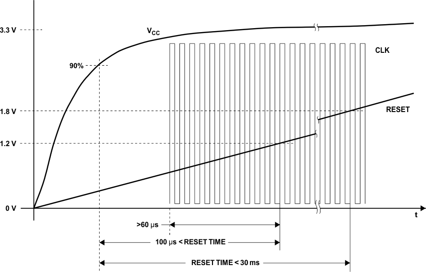
There are three requirements for the reset signal timing. First, the minimum reset pulse duration is 100 μs. At power up, this time is measured from the time the power ramps up to 90% of the nominal VCC until the reset signal exceeds 1.2 V. The second requirement is that the clock must be valid during the last 60 µs of the reset window. The third requirement is that, according to the USB specification, the device must be ready to respond to the host within 100 ms. This means that within the 100-ms window, the device must come out of reset, load any pertinent data from the I2C EEPROM device, and transfer execution to the application firmware if any is present. Because the latter two events can require significant time, the amount of which can change from system to system, TI recommends having the device come out of reset within 30 ms, leaving 70 ms for the other events to complete. This means the reset signal must rise to
1.8 V within 30 ms.
These requirements are depicted in Figure 4-1. When using a 12-MHz crystal, the clock signal may take several milliseconds to ramp up and become valid after power up. Therefore, the reset window may need to be elongated up to 10 ms or more to ensure that there is a 60-µs overlap with a valid clock.
 Figure 4-1 Reset Timing
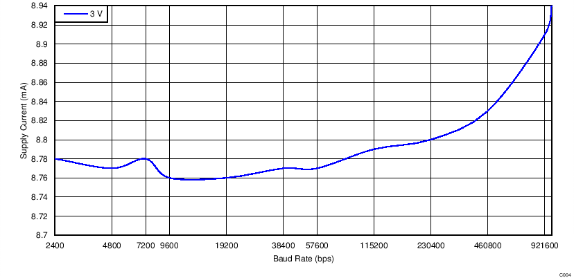
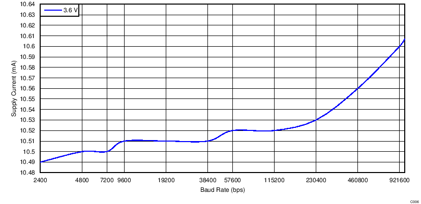
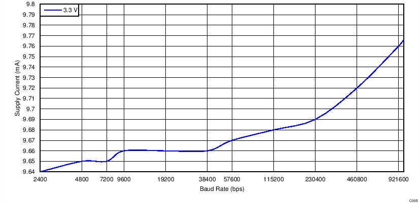
4.7 Typical Characteristics


