SLLS519J March 2002 – July 2017 TUSB3410
PRODUCTION DATA.
- 1Device Overview
- 2Revision History
- 3Pin Configuration and Functions
- 4Specifications
-
5Detailed Description
- 5.1 Overview
- 5.2 Functional Block Diagram
- 5.3 Device Functional Modes
- 5.4 Processor Subsystems
- 5.5
Memory
- 5.5.1 MCU Memory Map
- 5.5.2 Registers
- 5.5.3 Buffers + I/O RAM Map
- 5.5.4
Endpoint Descriptor Block (EDB−1 to EDB−3)
- 5.5.4.1 OEPCNF_n: Output Endpoint Configuration (n = 1 to 3) (Base Addr: FF08h, FF10h, FF18h)
- 5.5.4.2 OEPBBAX_n: Output Endpoint X-Buffer Base Address (n = 1 to 3) (Offset 1)
- 5.5.4.3 OEPBCTX_n: Output Endpoint X Byte Count (n = 1 to 3) (Offset 2)
- 5.5.4.4 OEPBBAY_n: Output Endpoint Y-Buffer Base Address (n = 1 to 3) (Offset 5)
- 5.5.4.5 OEPBCTY_n: Output Endpoint Y-Byte Count (n = 1 to 3) (Offset 6)
- 5.5.4.6 OEPSIZXY_n: Output Endpoint X-/Y-Buffer Size (n = 1 to 3) (Offset 7)
- 5.5.4.7 IEPCNF_n: Input Endpoint Configuration (n = 1 to 3) (Base Addr: FF48h, FF50h, FF58h)
- 5.5.4.8 IEPBBAX_n: Input Endpoint X-Buffer Base Address (n = 1 to 3) (Offset 1)
- 5.5.4.9 IEPBCTX_n: Input Endpoint X-Byte Count (n = 1 to 3) (Offset 2)
- 5.5.4.10 IEPBBAY_n: Input Endpoint Y-Buffer Base Address (n = 1 to 3) (Offset 5)
- 5.5.4.11 IEPBCTY_n: Input Endpoint Y-Byte Count (n = 1 to 3) (Offset 6)
- 5.5.4.12 IEPSIZXY_n: Input Endpoint X-/Y-Buffer Size (n = 1 to 3) (Offset 7)
- 5.5.4.13 Endpoint-0 Descriptor Registers
- 5.5.5
USB Registers
- 5.5.5.1 FUNADR: Function Address Register (Addr:FFFFh)
- 5.5.5.2 USBSTA: USB Status Register (Addr:FFFEh)
- 5.5.5.3 USBMSK: USB Interrupt Mask Register (Addr:FFFDh)
- 5.5.5.4 USBCTL: USB Control Register (Addr:FFFCh)
- 5.5.5.5 MODECNFG: Mode Configuration Register (Addr:FFFBh)
- 5.5.5.6 Clock Output Control
- 5.5.5.7 Vendor ID/Product ID
- 5.5.5.8 SERNUM7: Device Serial Number Register (Byte 7) (Addr:FFEFh)
- 5.5.5.9 SERNUM6: Device Serial Number Register (Byte 6) (Addr:FFEEh)
- 5.5.5.10 SERNUM5: Device Serial Number Register (Byte 5) (Addr:FFEDh)
- 5.5.5.11 SERNUM4: Device Serial Number Register (Byte 4) (Addr:FFECh)
- 5.5.5.12 SERNUM3: Device Serial Number Register (Byte 3) (Addr:FFEBh)
- 5.5.5.13 SERNUM2: Device Serial Number Register (Byte 2) (Addr:FFEAh)
- 5.5.5.14 SERNUM1: Device Serial Number Register (Byte 1) (Addr:FFE9h)
- 5.5.5.15 SERNUM0: Device Serial Number Register (Byte 0) (Addr:FFE8h)
- 5.5.5.16 Function Reset and Power-Up Reset Interconnect
- 5.5.5.17 Pullup Resistor Connect and Disconnect
- 5.5.6
DMA Controller Registers
- 5.5.6.1 DMACDR1: DMA Channel Definition Register (UART Transmit Channel) (Addr:FFE0h)
- 5.5.6.2 DMACSR1: DMA Control And Status Register (UART Transmit Channel) (Addr:FFE1h)
- 5.5.6.3 DMACDR3: DMA Channel Definition Register (UART Receive Channel) (Addr:FFE4h)
- 5.5.6.4 DMACSR3: DMA Control And Status Register (UART Receive Channel) (Addr:FFE5h)
- 5.5.7
UART Registers
- 5.5.7.1 RDR: Receiver Data Register (Addr:FFA0h)
- 5.5.7.2 TDR: Transmitter Data Register (Addr:FFA1h)
- 5.5.7.3 LCR: Line Control Register (Addr:FFA2h)
- 5.5.7.4 FCRL: UART Flow Control Register (Addr:FFA3h)
- 5.5.7.5 Transmitter Flow Control
- 5.5.7.6 MCR: Modem-Control Register (Addr:FFA4h)
- 5.5.7.7 LSR: Line-Status Register (Addr:FFA5h)
- 5.5.7.8 MSR: Modem-Status Register (Addr:FFA6h)
- 5.5.7.9 DLL: Divisor Register Low Byte (Addr:FFA7h)
- 5.5.7.10 DLH: Divisor Register High Byte (Addr:FFA8h)
- 5.5.7.11 Baud-Rate Calculation
- 5.5.7.12 XON: Xon Register (Addr:FFA9h)
- 5.5.7.13 XOFF: Xoff Register (Addr:FFAAh)
- 5.5.7.14 MASK: UART Interrupt-Mask Register (Addr:FFABh)
- 5.5.8 Expanded GPIO Port
- 5.5.9 Interrupts
- 5.5.10 I2C Registers
- 5.6
Boot Modes
- 5.6.1 Introduction
- 5.6.2 Bootcode Programming Flow
- 5.6.3 Default Bootcode Settings
- 5.6.4 External I2C Device Header Format
- 5.6.5 Checksum in Descriptor Block
- 5.6.6 Header Examples
- 5.6.7 USB Host Driver Downloading Header Format
- 5.6.8 Built-In Vendor Specific USB Requests
- 5.6.9 Bootcode Programming Consideration
- 5.6.10 File Listings
- 6Application, Implementation, and Layout
- 7Device and Documentation Support
- 8Mechanical Packaging and Orderable Information
封裝選項
機械數據 (封裝 | 引腳)
散熱焊盤機械數據 (封裝 | 引腳)
- RHB|32
訂購信息
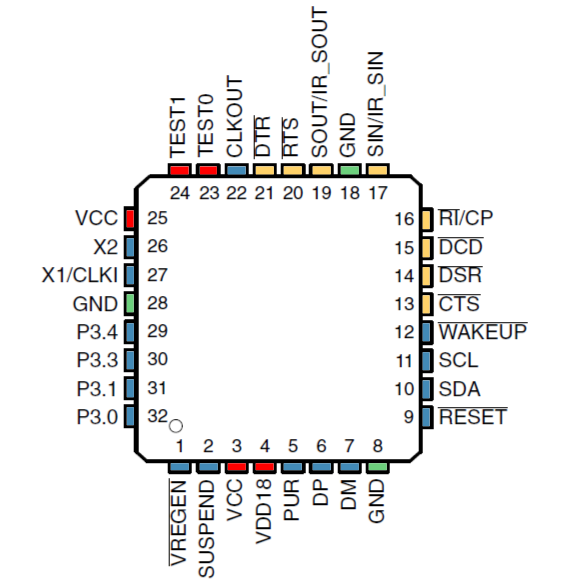
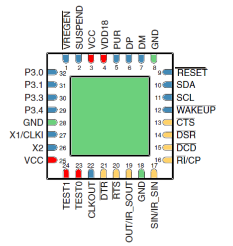
3 Pin Configuration and Functions
3.1 Pin Diagrams
RHB Package
32-Pin VQFN
Top View

VF Package
32-Pin LQFP
Bottom View

Pin Functions
| PIN | I/O | DESCRIPTION | |
|---|---|---|---|
| NAME | NO. | ||
| CLKOUT | 22 | O | Clock output (controlled by bits 2 (CLKOUTEN) and 3(CLKSLCT) in the MODECNFG register (see (1) and Section 5.5.5.5) |
| CTS | 13 | I | UART: Clear to send(4) |
| DCD | 15 | I | UART: Data carrier detect(4) |
| DM | 7 | I/O | Upstream USB port differential data minus |
| DP | 6 | I/O | Upstream USB port differential data plus |
| DSR | 14 | I | UART: Data set ready(4) |
| DTR | 21 | O | UART: Data terminal ready(1) |
| GND | 8, 18, 28 | GND | Digital ground |
| P3.0 | 32 | I/O | General-purpose I/O 0 (port 3, terminal 0)(3)(5)(8) |
| P3.1 | 31 | I/O | General-purpose I/O 1 (port 3, terminal 1)(3)(5)(8) |
| P3.3 | 30 | I/O | General-purpose I/O 3 (port 3, terminal 3)(3)(5)(8) |
| P3.4 | 29 | I/O | General-purpose I/O 4 (port 3, terminal 4)(3)(5)(8) |
| PUR | 5 | O | Pullup resistor connection(2) |
| RESET | 9 | I | Device master reset input(4) |
| RI/CP | 16 | I | UART: Ring indicator(4) |
| RTS | 20 | O | UART: Request to send(1) |
| SCL | 11 | O | Master I2C controller: clock signal(1) |
| SDA | 10 | I/O | Master I2C controller: data signal(1)(5) |
| SIN/IR_SIN | 17 | I | UART: Serial input data / IR Serial data input(6) |
| SOUT/IR_SOUT | 19 | O | UART: Serial output data / IR Serial data output(7) |
| SUSPEND | 2 | O | Suspend indicator terminal(3). When this terminal is asserted high, the device is in suspend mode. |
| TEST0 | 23 | I | Test input (for factory test only). This terminal must be tied to VCC through a 10-kΩ resistor. |
| TEST1 | 24 | I | Test input (for factory test only)(5). This terminal must be tied to VCC through a 10-kΩ resistor. |
| VCC | 3, 25 | PWR | 3.3 V |
| VDD18 | 4 | PWR | 1.8-V supply. An internal voltage regulator generates this supply voltage when terminal VREGEN is low. When VREGEN is high, 1.8 V must be supplied externally. |
| VREGEN | 1 | I | This active-low terminal is used to enable the 3.3-V to 1.8-V voltage regulator. |
| WAKEUP | 12 | I | Remote wake-up request terminal. When low, wakes up system(5) |
| X1/CLKI | 27 | I | 12-MHz crystal input or clock input |
| X2 | 26 | O | 12-MHz crystal output |
(1) 3-state CMOS output (±4-mA drive and sink)
(2) 3-state CMOS output (±8-mA drive and sink)
(3) 3-state CMOS output (±12-mA drive and sink)
(4) TTL-compatible, hysteresis input
(5) TTL-compatible, hysteresis input, with internal 100-µA active pullup resistor
(6) TTL-compatible input without hysteresis, with internal 100-µA active pullup resistor
(7) Normal or IR mode: 3-state CMOS output (±4-mA drive and sink)
(8) The MCU treats the outputs as open drain types in that the output can be driven low continuously, but a high output is driven for two clock cycles and then the output is high impedance.