SLVAE85A February 2019 – September 2025 LM1117-Q1 , LM317 , LP2951 , LP2951-Q1 , LP2985 , TL1963A , TL1963A-Q1 , TLV1117 , TLV709 , TLV755P , TLV761 , TLV766-Q1 , TLV767 , TLV767-Q1 , TPS709 , TPS709-Q1 , TPS715 , TPS745 , TPS7A16A , TPS7A16A-Q1 , TPS7A25 , TPS7A26 , TPS7A43 , TPS7A44 , TPS7A47 , TPS7A47-Q1 , TPS7A49 , TPS7B63-Q1 , TPS7B68-Q1 , TPS7B69-Q1 , TPS7B81 , TPS7B81-Q1 , TPS7B82-Q1 , TPS7B83-Q1 , TPS7B84-Q1 , TPS7B85-Q1 , TPS7B86-Q1 , TPS7B87-Q1 , TPS7B88-Q1 , TPS7B91 , TPS7B92 , TPS7C84-Q1 , UA78L , UA78M , UA78M-Q1
- 1
- An empirical analysis of the impact of board layout on LDO thermal performance
- Trademarks
- 1Introduction
- 2Procedure
- 3Test Results and Discussion
- 4Conclusion
- 5Future Study
- 6References
- 7Revision History
- A Thermal Test Board Layouts
- B Thermal Test Results
3 Test Results and Discussion
Figure 3-1 shows the maximum ambient temperature versus power dissipation for the TPS745 (WSON package) in the 1S0P Approximation layout. The slope of the trendline indicates a θJA of 169.2 C/W. The range and linearity of the data collected support the expected relationship between the power dissipation of the LDO and the maximum operating ambient temperature described by Equation 2.
 1S0P Approximation Layout Test Results") Figure 3-1 TPS745 (WSON) 1S0P Approximation Layout Test Results
Figure 3-1 TPS745 (WSON) 1S0P Approximation Layout Test ResultsSee Appendix B for similar data is collected for all packages and layouts. Figure 3-2 and Figure 3-3 provide the resulting θJA values for the TPS745 (WSON) and TPS7B82-Q1 (TO-252). These packages display similar trends in thermal performance across all five layouts. The Internally Disconnected layout reduces θJA by almost 50% despite only having a connected copper area of 0.07-in2, showing that including copper on the internal layers can significantly improve thermal performance, even if this copper is not directly connected to the LDO. The remaining layouts with increasing copper and thermal vias content show further, smaller reductions of θJA until the maximum reduction is reached at slightly larger than 70%. Based on the data collected, a thermally efficient layout is crucial for the WSON and TO-252 packages. If the layout is inefficient, θJA is significantly larger than the datasheet specified value, resulting in more complex thermal performance calculations, a reduced maximum operating ambient temperature, and potentially degraded device longevity and reliability.
 θJA vs. Board Layout") Figure 3-2 TPS745 (WSON) θJA vs. Board Layout
Figure 3-2 TPS745 (WSON) θJA vs. Board Layout θJA vs. Board Layout") Figure 3-3 TPS7B82-Q1 (TO-252) θJA vs. Board Layout
Figure 3-3 TPS7B82-Q1 (TO-252) θJA vs. Board LayoutFigure 3-4 shows the measured θJA values for the TLV755P (SOT-23). The difference in the θJA trend for the SOT-23 package is due to the lack of a thermal pad. The JEDEC standard does not permit the addition of thermal vias on the High-K Thermal Test Board for packages without thermal pads. A small amount of heat is able to dissipate to the internal and bottom layers, resulting in very similar performance between the 1S0P Approximation and the thermal model of the JEDEC High-K Test Board from which the datasheet specification is derived. To prevent identical performance across multiple different layouts, one thermal via is included underneath the device on the Internally Disconnected layout to connect the top layer ground trace to the bottom ground plane. In comparison, the JEDEC High-K Approximation layout has similar performance with two vias connecting the top ground trace to the internal layers. Adding one more via does not provide enough heat transferring capability to warrant much improvement in θJA despite the additional copper present in the JEDEC High-K Approximation layout.
The Thermally Enhanced and Thermally Saturated boards displayed about a 33% reduction to θJA compared to the JEDEC High-K Approximation board, significantly larger than the same comparison for the TPS745 and TPS7B82-Q1. This is explained by the lack of a thermal pad in the SOT-23 package. The Thermally Enhanced and Thermally Saturated layouts are the only layouts that include copper planes on the top layer. The lack of a thermal pad in this package results in the majority of heat dissipating on the top layer. As such, the inclusion of top layer copper is much more effective. Furthermore, the additional thermal vias included in the Thermally Enhanced and Thermally Saturated packages are the only path for heat to spread to the internal and bottom layers. In contrast, the TPS745 and TPS7B82-Q1 layouts include thermal vias directly under the thermal pad, reducing the effectiveness of additional thermal vias.
 θJA vs. Board Layout") Figure 3-4 TLV755P (SOT-23) θJA vs. Board Layout
Figure 3-4 TLV755P (SOT-23) θJA vs. Board LayoutFigure 3-5 compares the effectiveness of PCB layout versus the package type. The effectiveness is calculated as a percentage reduction of θJA. As calculated with Equation 3, a thermally efficient layout is capable of reducing the θJA specified in the datasheet by between 32% and 55% depending on the package. The datasheet specified θJA can be used to provide a conservative estimate of the rise in junction temperature of the LDO. However, referring to Equation 2, the empirical rise in junction temperature can be reduced by 32% to 55% with a thermally efficient layout. Accounting for this improvement allows for a higher operating ambient temperature, a higher level of power dissipation, or some combination of the two. A comparison to the 1S0P Approximation layout using Equation 4 illustrates the importance of a thermally efficient layout. Compared to this worst-case layout, a thermally efficient layout provides a measured θJA that is up to four times smaller.

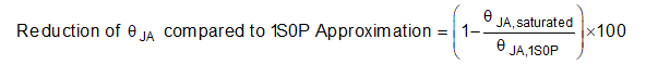
 Figure 3-5 θJA Reduction for Each Device
Figure 3-6 normalizes the results from the Figure 3-2, Figure 3-3, and Figure 3-4 relative to the datasheet specification using Equation 5.
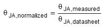
This figure condenses the data collected across the three packages to illustrate the important findings of this study. Firstly, there is an inverse relationship between PCB copper content and θJA that saturates as the copper content increases. This relationship is observable regardless of package. As shown by the significant drop between the 1S0P Approximation and Internally Disconnected layouts, the copper content does not need to be connected to the LDO to improve thermal performance. Additional thermal vias around the device also improve thermal performance by providing more paths for the heat generated by the LDO to dissipate to the internal and bottom layers. These vias are especially important for packages like the SOT-23 that do not have a dedicated thermal pad. However, as shown by the minimal improvement between the Thermally Enhanced and Thermally Saturated layouts, the improvement in θJA from the additional thermal vias saturates.
 Figure 3-6 Normalized θJA for Each Device vs. Board Layout