SLVUDF6 September 2025
4.1.1 Equipment Setup
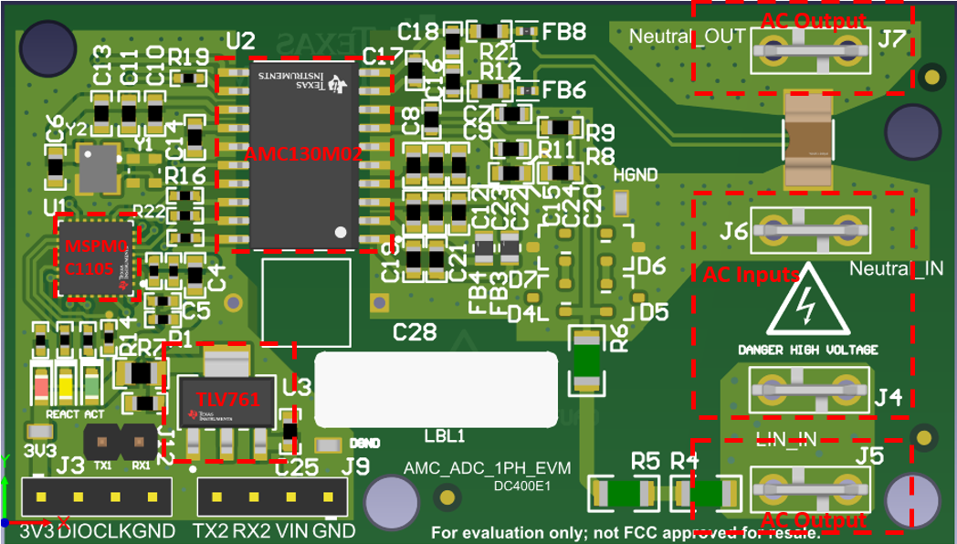
Figure 4-1shows the location of various components of the reference design on the top layer of the PCB. The bottom layer has no soldered components.
 Figure 4-1 AMC-ADC-1PH-EVM Hardware 3D View
Table 4-1 lists the jumper settings.
Table 4-1 Hardware Jumper Settings
| HEADER NAME | TYPE | MAIN FUNCTIONALITY | COMMENTS |
|---|---|---|---|
| J3 | 4 pin | JTAG: MSPM0 programming header | |
| J4, J6 | 1 pin | Positive and negative AC input header | Connect AC Line and Neutral to J5 J6 |
| J5, J7 | 1 pin | Positive and negative AC output header | Connect load the J4 J7 |
| J9 | 4 pin | UART output to connect to main controller and External power supply | |
| J12 | 2 pin | UART to connect with PC GUI |