SLUSFS4A September 2025 – September 2025 UCC27734-Q1 , UCC27735-Q1
PRODUCTION DATA
- 1
- 1 Features
- 2 Applications
- 3 Description
- 4 Pin Configuration and Functions
- 5 Specifications
-
6 Detailed Description
- 6.1 Overview
- 6.2 Functional Block Diagram
- 6.3
Feature Description
- 6.3.1 Input Stages and Interlock
- 6.3.2 Enable Function (UCC277x5-Q1 Only)
- 6.3.3 Undervoltage Lockout (UVLO)
- 6.3.4 Level Shifter
- 6.3.5 Output Stage
- 6.3.6 Low Propagation Delays and Tightly Matched Outputs
- 6.3.7 HS Node dV/dt
- 6.3.8 Split Grounds (COM and VSS)
- 6.3.9 Operation Under Negative HS Voltage Condition
- 6.4 Device Functional Modes
-
7 Application and Implementation
- 7.1 Application Information
- 7.2
Typical Application
- 7.2.1 Design Requirements
- 7.2.2
Detailed Design Procedure
- 7.2.2.1 Selecting HI and LI Low Pass Filter Components (RHI, RLI, CHI, CLI)
- 7.2.2.2 Selecting Bootstrap Capacitor (CBOOT)
- 7.2.2.3 Selecting VDD Bypass Capacitor (CVDD)
- 7.2.2.4 Selecting Bootstrap Resistor (RBOOT)
- 7.2.2.5 Selecting Gate Resistor RHO/RLO
- 7.2.2.6 Selecting Bootstrap Diode
- 7.2.2.7 Estimate the UCC2773x-Q1 Power Losses
- 7.2.2.8 Application Example Schematic Note
- 7.2.3 Application Curves
- 7.3 Power Supply Recommendations
- 7.4 Layout
- 8 Device and Documentation Support
- 9 Revision History
- 10Mechanical, Packaging, and Orderable Information
封裝選項(xiàng)
機(jī)械數(shù)據(jù) (封裝 | 引腳)
- D|14
散熱焊盤機(jī)械數(shù)據(jù) (封裝 | 引腳)
訂購信息
6.3.9 Operation Under Negative HS Voltage Condition
A typical half-bridge configuration with the UCC2773x-Q1 is shown in Figure 6-5. There are parasitic inductances in the power circuit from die bonding and pinning in QT/QB and PCB tracks of power circuit, the parasitic inductances are labeled LK1,2,3,4.
During switching of HS, the current path of power circuit is changed to current path 2 from current path 1. This is known as current commutation. The current across LK3, LK4 and body diode of QB pulls HS lower than COM, like shown in the waveform in Figure 6-5. However, the UCC2773x-Q1 offers robust operation under these conditions of negative voltage on HS.
 Figure 6-5 HS Negative
Voltage In Half-Bridge Configuration
Figure 6-5 HS Negative
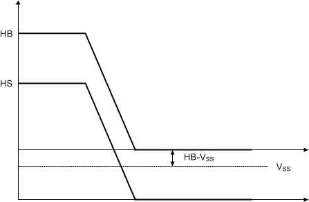
Voltage In Half-Bridge ConfigurationThe level shifter circuit is referenced to COM/VSS (refer to Section 6.2), the voltage from HB to COM/VSS is the supply voltage of the level shifter. When HS is a negative voltage with respect to COM/VSS, the voltage of HB–(COM/VSS) is decreased, as shown in Figure 6-6. There is a minimum operational supply voltage of the level shifter, if the supply voltage of level shifter is too low, the level shifter cannot pass the HI signal to HO. The minimum supply voltage of the level shifter of the UCC2773x-Q1 is 3V, so the recommended HS specification is dependent on HB-HS. The specification of minimum recommended HS is –9V at HB – HS = 12V.
In general, HS can operate until -9V when HB – HS = 12V. If HB–HS voltage is different, the minimum HS voltage changes accordingly.
 Figure 6-6 Level Shifter
Supply Voltage with Negative HS
Figure 6-6 Level Shifter
Supply Voltage with Negative HSLogic operational for HS greater than –9V to 600V at HB – HS = 12V
The capability of a typical UCC2773x-Q1 device to operate under a negative voltage condition on the HS pin is reported in Figure 6-8. The test method is shown in Figure 6-7.
 Figure 6-7 Negative Voltage Test Method
 Figure 6-8 NTSOA (Negative
Transient Safe Operating Area) Maximum Negative HS Voltage vs Pulse Width
 The above curve is a typical curve based on limited units tested at 25°C and at VHB –VHS= 12V. The curve gives a general guideline as to what negative transients the device can survive, but it is still recommended to limit the negative transients to within the device recommended specifications through layout and design.